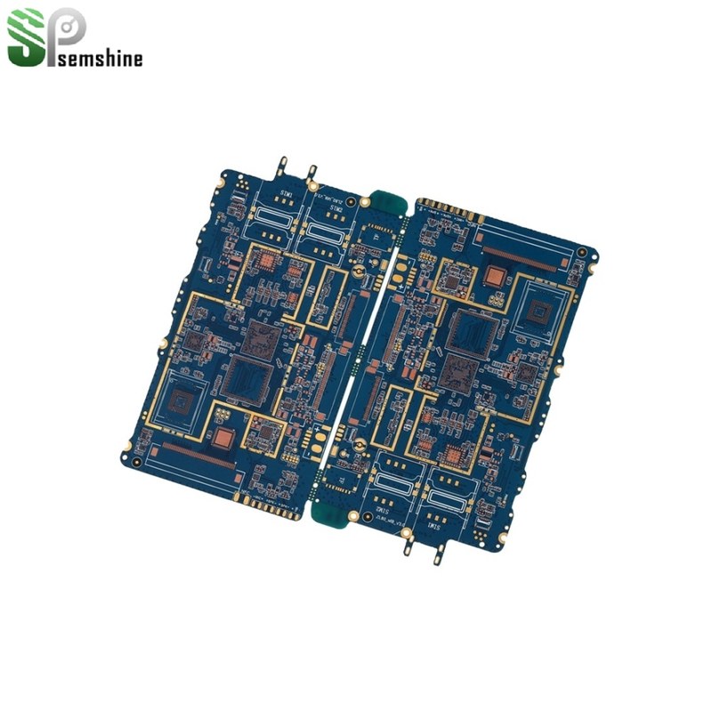
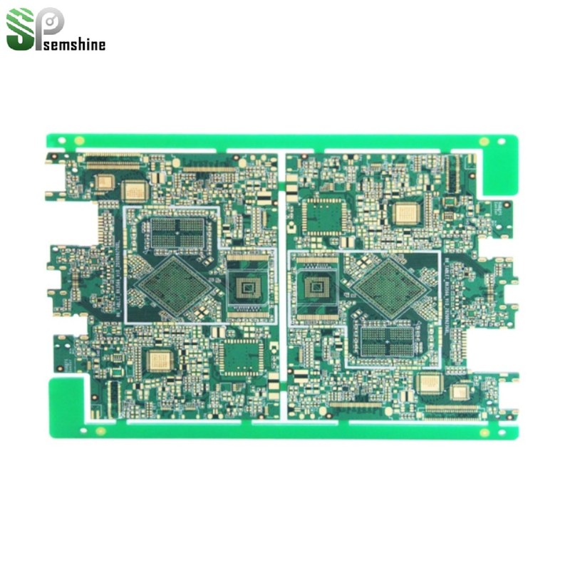
HDI PCBs employ advanced technologies and manufacturing processes to minimize the size of the circuit board and provide higher routing density. They typically utilize multilayer construction with micro-sized traces, fine pitch, and the use of blind vias and buried vias to achieve highly integrated circuit layouts.
HDI PCBs offer several advantages. Firstly, they allow for more electronic components to be accommodated in a smaller space, providing higher functional density. Secondly, HDI PCBs provide shorter signal paths, lower resistance, and inductance, improving signal integrity and performance. Additionally, HDI PCBs exhibit better resistance to interference and higher reliability. We're a professional HDI PCB manufacturer, produce HDI printed circuit boards with laser blind, buried and stacked microvias, customizable with high TG, halogen-free substrate, impedance control and ENIG/HASL/OSP/Immersion Silver surface finishes. HDI technology realizes ultra-high wiring density and miniaturization, widely used in smartphones, wearable devices, 5G communication, automotive electronics, medical equipment and high-end consumer electronics, all with UL, RoHS and REACH certifications.
| Product Parameters | |
|---|---|
| PCB description | |
| Model Number | HighTG HDI PCB |
| Place of Origin | Shenzhen, China |
| Base Material | FR4 |
| Layers | 12 L |
| Copper Thickness | 1oz |
| Board Thickness | 1.6mm |
| Min. Hole Size | 0.15mm |
| Min. Line Width | 3 Mil |
| Min. Line Spacing | 0.1um(3 Mil) |
| Surface Finishing | ENIG |
| Color | Green Solder mask and White silkscreen |