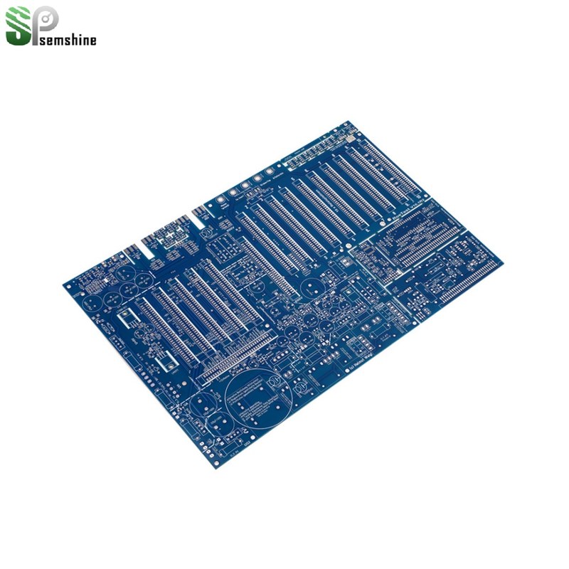
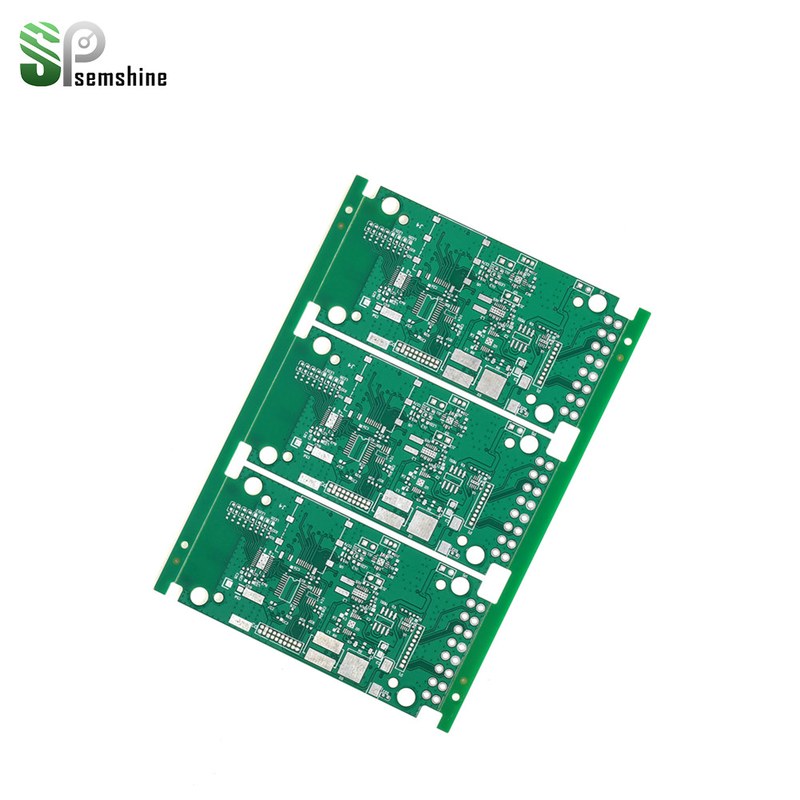
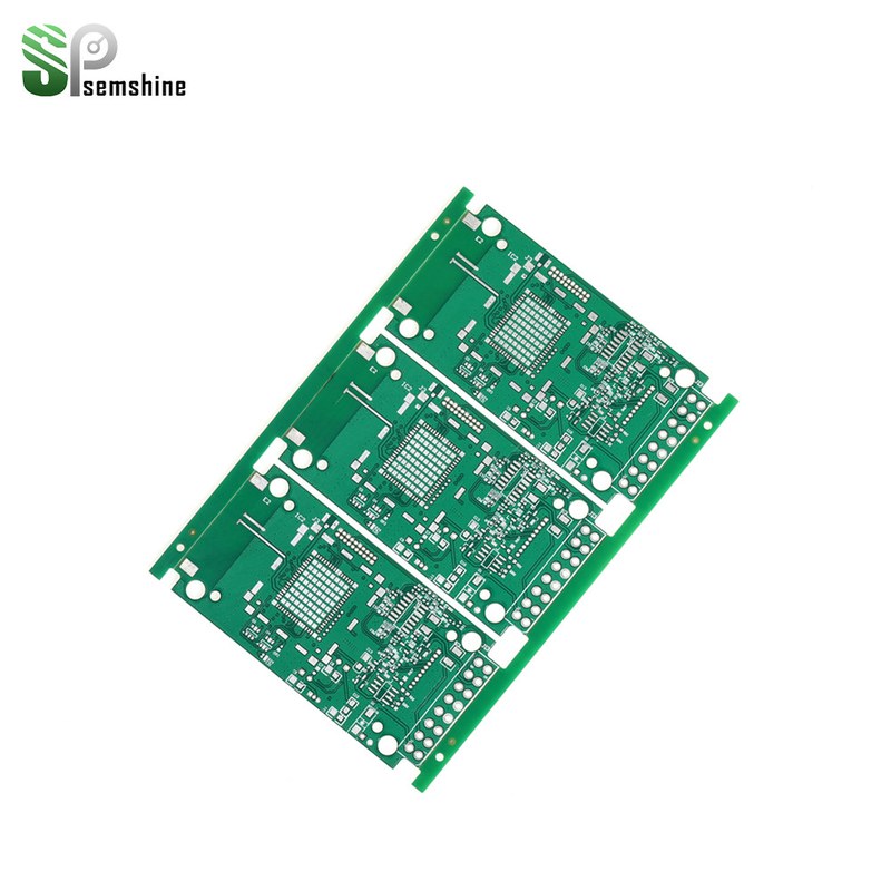
Multilayer PCB (Printed Circuit Board) refers to a type of PCB that consists of multiple layers of conductive traces and insulating material stacked together. Unlike single-layer or double-layer PCBs, which have only one or two layers of conductive material, multilayer PCBs provide increased design flexibility and complexity by incorporating multiple layers.
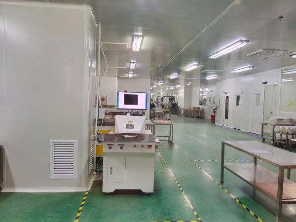
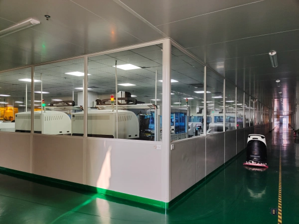
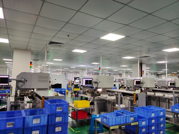
In a multilayer PCB, the layers are interconnected using vias, which are small plated holes that allow electrical connections between the different layers. These vias can be through-hole vias, which traverse through all the layers, or they can be blind vias, which connect one or more inner layers but do not traverse the entire board, or buried vias, which connect inner layers without being exposed on the outer layers. We are a professional multi-layer PCB manufacturer, customizable with high TG, heavy copper, blind & buried vias, impedance control, gold fingers and various surface finishes (ENIG, HASL, OSP, Immersion Silver). All boards pass UL, RoHS and REACH certifications, widely applied in automotive electronics, medical devices, 5G communication, industrial automation, new energy storage and consumer high-end electronics.
| Product Parameters | |
|---|---|
| PCB description | |
| Model Number | 6-layer PCB |
| Place of Origin | Shenzhen, China |
| Base Material | FR4 TG170 |
| Layers | 6L |
| Copper Thickness | 2oz |
| Board Thickness | 1.6mm |
| Min. Hole Size | 0.15mm |
| Min. Line Width | 3 Mil |
| Min. Line Spacing | 3 Mil |
| Surface Finishing | HASL |
| Color | Green Solder mask and White silkscreen |