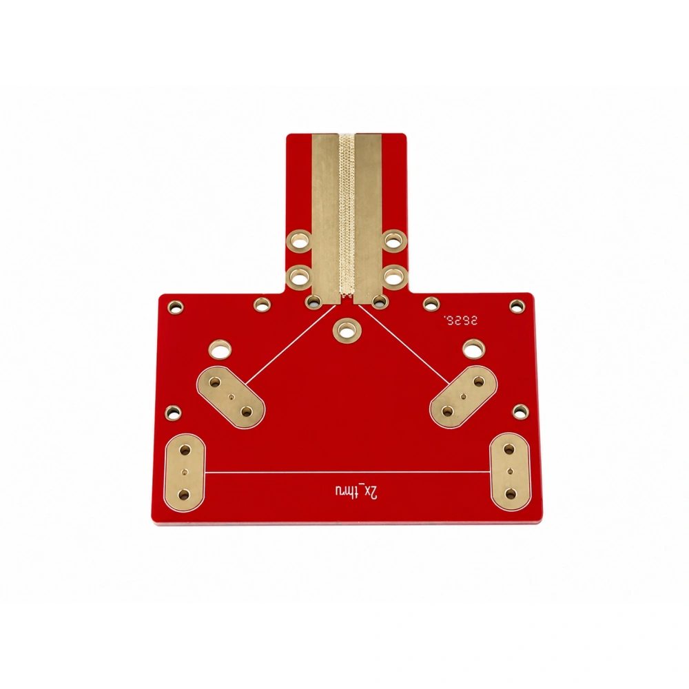
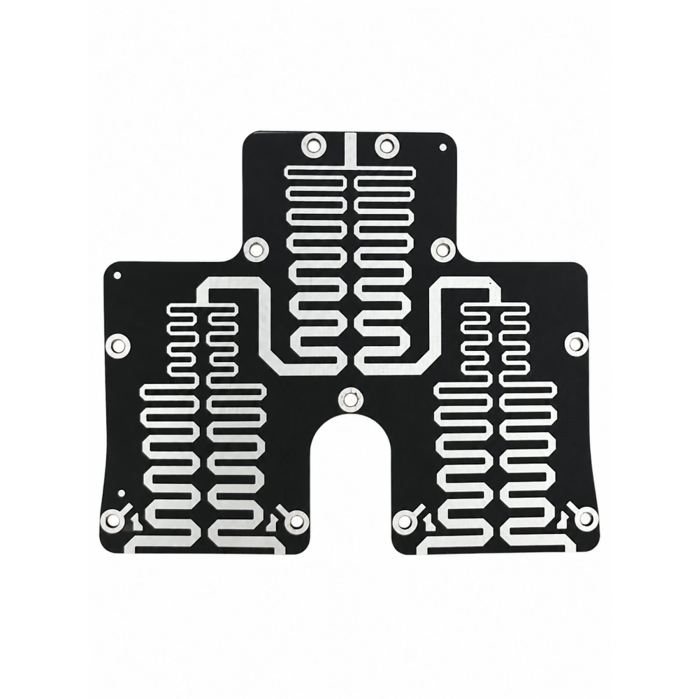
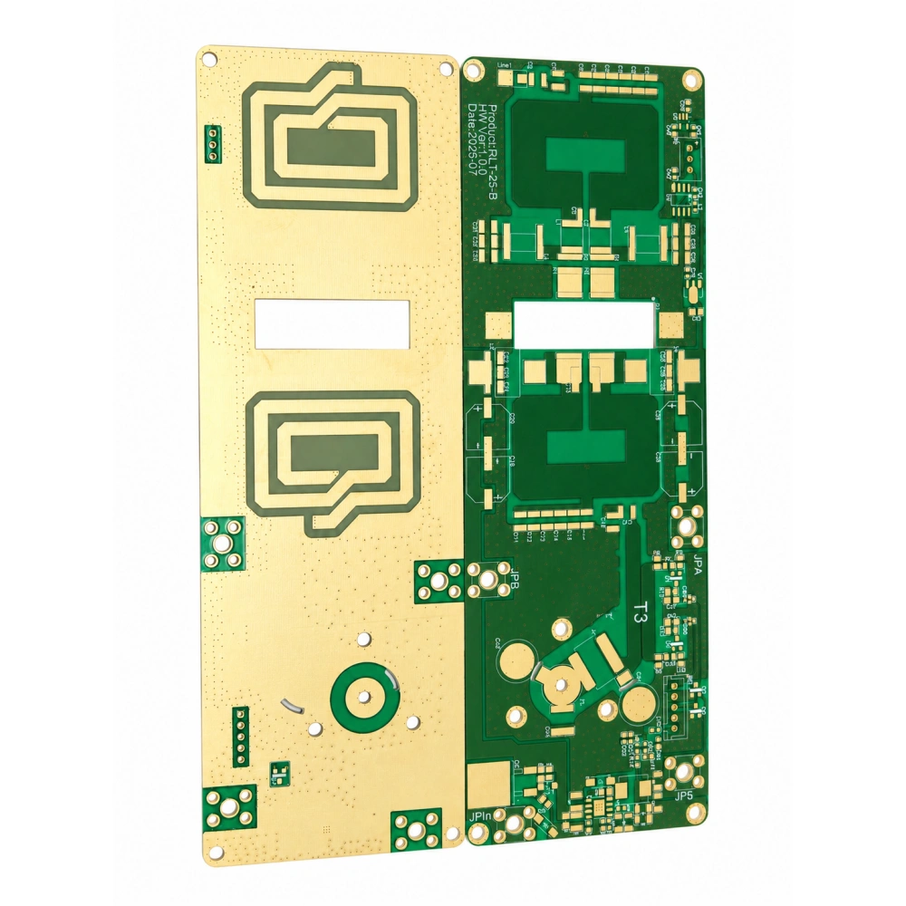
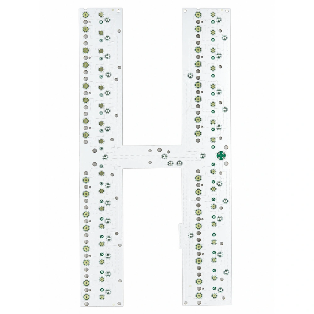
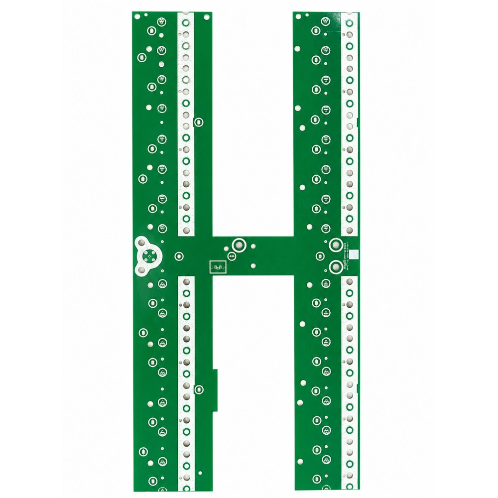
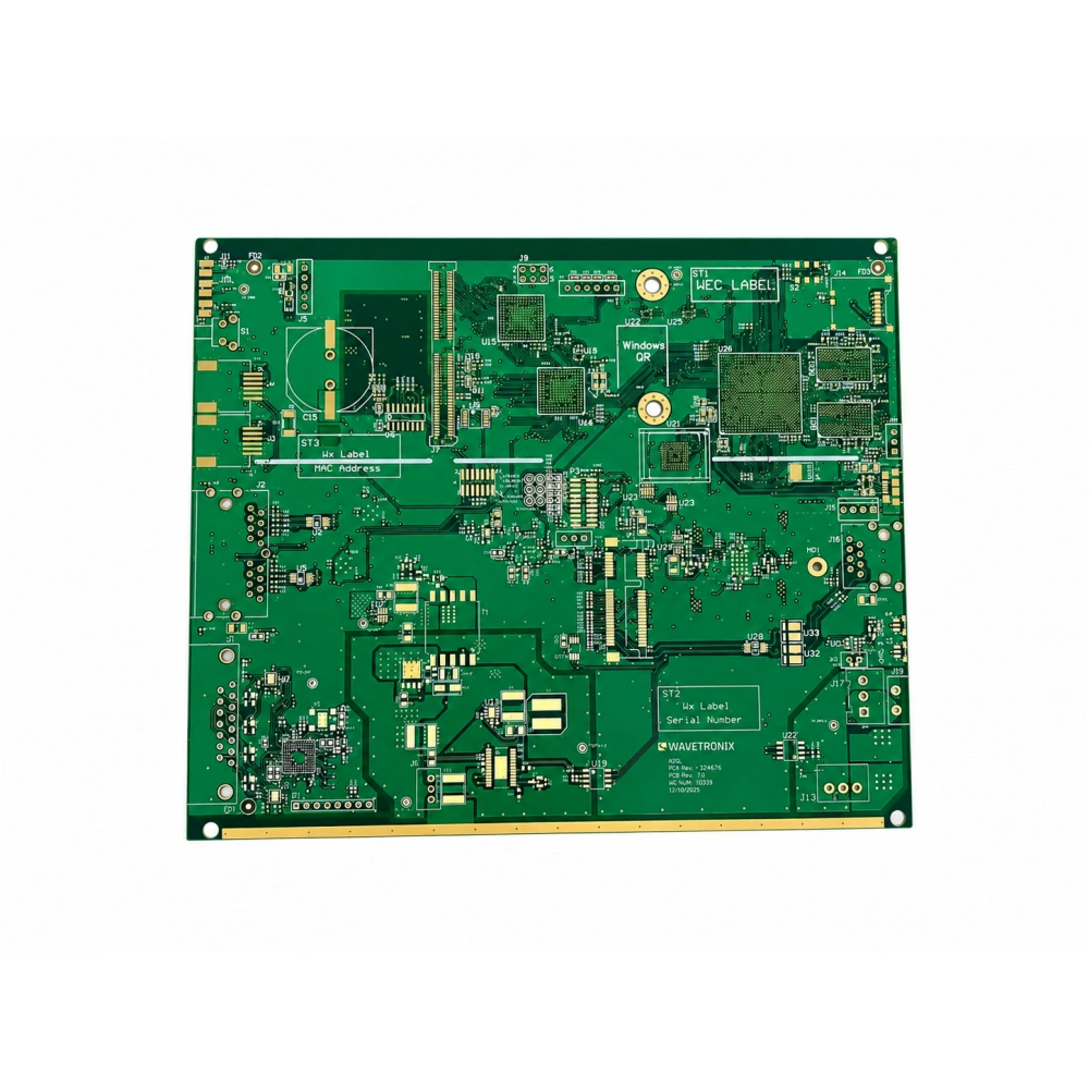
High-Frequency PCB for RF, Microwave and High-Speed Applications
High-frequency PCB technology is essential for electronic systems that operate at elevated frequencies and require stable signal transmission, low dielectric loss, and precise electrical performance. Unlike conventional FR-4 circuit boards, high-frequency PCB materials are specifically engineered to maintain consistent electrical characteristics as signal frequencies increase. SEMSHINE provides customized high-frequency PCB solutions for demanding RF, microwave, wireless communication, radar, automotive electronics, telecommunications, and other high-speed applications where signal integrity and reliability are critical.
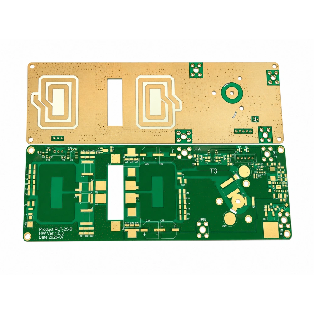
Our high-frequency PCB manufacturing capabilities support a wide range of specialized materials, including Rogers materials and other low-loss laminates selected according to the electrical and mechanical requirements of each project. Rogers PCB solutions are particularly suitable for applications where controlled dielectric properties, low signal loss, and stable impedance are required. Depending on the design, materials such as Rogers RO4350B, RO4003C, RO3003 and other high-frequency laminates can be used to achieve the required electrical performance. For cost-sensitive designs, hybrid constructions combining high-frequency materials with conventional FR-4 can also be considered.
A major advantage of a high-frequency PCB is its ability to maintain predictable signal behavior at high operating frequencies. Material properties such as dielectric constant (Dk), dissipation factor (Df), thermal performance, and dimensional stability directly influence signal propagation and overall circuit performance. Our manufacturing process therefore focuses on material selection, stack-up design, controlled impedance, copper pattern accuracy, dielectric thickness, and lamination control. These factors are carefully considered during engineering review before production begins.
For RF and microwave circuits, even small variations in trace width, dielectric thickness, copper surface characteristics, or layer registration can affect impedance and signal performance. Our engineering team reviews the PCB fabrication data and manufacturing requirements to identify potential production risks and ensure that critical specifications are clearly defined. Controlled impedance requirements can be incorporated into the PCB manufacturing process, with appropriate trace geometry and dielectric structures selected according to the target impedance values.
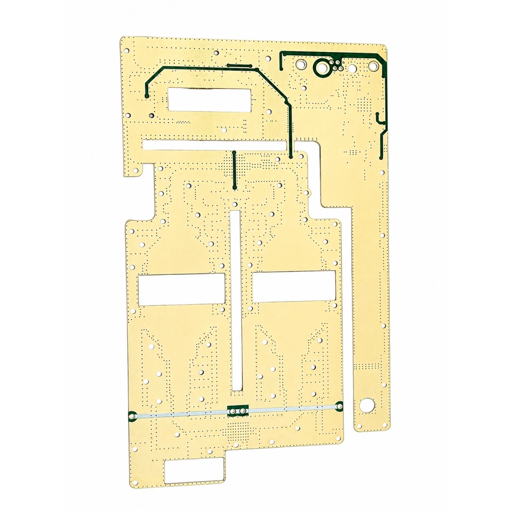
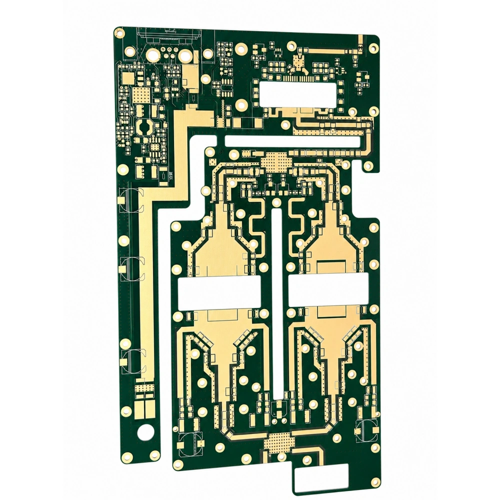
SEMSHINE also supports multilayer high-frequency PCB designs with complex stack-ups and mixed-material constructions. Depending on the application, boards can be manufactured with different layer counts, copper weights, surface finishes, via structures, and board thicknesses. When a project combines high-frequency performance with high routing density, the high-frequency PCB can also incorporate advanced interconnection technologies such as blind vias, buried vias, and microvias.
These circuit boards are widely used in RF modules, antennas, wireless communication equipment, 5G infrastructure, satellite communication systems, radar equipment, automotive radar, navigation systems, power amplifiers, test instruments, and other electronic products operating at high frequencies. For high-speed digital applications, low-loss PCB materials can also help reduce signal attenuation and improve signal integrity over high-speed transmission paths.
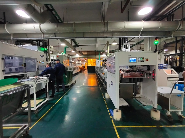
From prototype quantities to volume production, SEMSHINE provides high-frequency PCB manufacturing with engineering support throughout the production process. Each project can be customized according to material requirements, layer structure, impedance specifications, dimensions, copper thickness, surface finish, and application environment. By combining specialized high-frequency materials with controlled manufacturing processes, we help customers develop reliable RF, microwave, and high-speed circuit boards for demanding electronic applications.
| Product Parameters | |
|---|---|
| PCB description | |
| Model Number | High‑Frequency PCB |
| Place of Origin | Shenzhen, China |
| Base Material | Rogers |
| Layers | 6L |
| Copper Thickness | 0.5oz |
| Board Thickness | 1.75mm |
| Min. Hole Size | 0.15mm |
| Min. Line Width | 3 Mil |
| Min. Line Spacing | 0.1um(3 Mil) |
| Surface Finishing | Immersion silver |
| Color | Green Solder mask and White silkscreen |